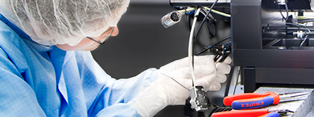

Wafer and chip inspection / measurement
For you we find customized solutions for non-contact optical inspection of wafers, probe cards, dies and microchip components. For this purpose, we offer systems for layer thickness measurement, contact inspection, electrical characterization, probe head positioning, sample manipulation and metrology of wafer microstructures in the nanometer range.
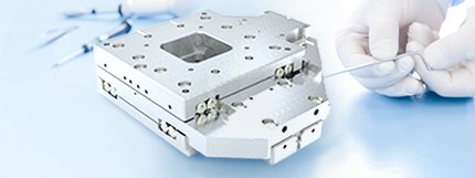
Custom Positioning Systems
 | travel 305 x 305 x 200 mm")
 | Stroke 720 x 720 x 100 mm")
 | Stroke 200 x 200 mm")
 | travel XYZ 30 x 30 x 20 mm, RxRy 4°, Rz 360°")

 | Stroke 720 x 720 x 100 mm")


 | rotary axis and linear stage")
")

Multi Axes Systems


 | Tripod, Rotary Stage, XY- Stage, Hexapod Alternative | Travel XYZ 30 x 30 x 20 mm, RxRy 4°, Rz 360°")


 | XY linear motor, profile rail | Phi belt, DC Motor | Travel 300 x 300 mm x 360°")
 | XY linear motor, profile rail | Z cross roller, ball screw drive | Phi belt, DC motor | Travel 450 x 350 x 16 mm x 45°")
 | XY linear motor, profile rail | Phi DC Motor | Travel 200 x 250 mm x 360°")
Standard Axes & Stages


Vacuum / Cleanroom


Ball & Lead Screw Drives


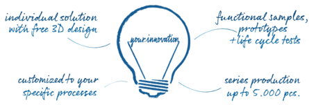
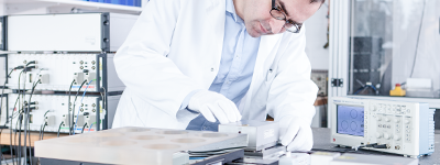
Individual customization and development of your Innovaiton
- Optimal positioning solution for your application with a fast and free 3D design
- Design of functional samples, prototypes up to series production
- Integrated development of your mechanics, electronics and software
Series production of your innovation on > 3.900 m² production area
more about the technical specifications